This convertor is designed to help engineers and PCB designers determine the exact width of a microstrip trace needed to achieve a desired characteristic impedance on a PCB.
Uses of Microstrip Width Convertor
1. Designing controlled impedance PCB traces.
2. Optimizing high-frequency circuit layouts.
3. Calculating width for RF and microwave signal traces.
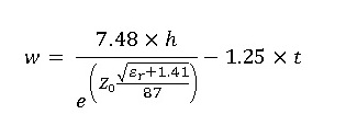

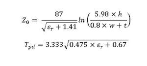
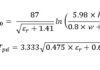
Conversion Formula
W = (7.48 × H) / exp( Z0 × √(εr + 1.41) / 87 ) − 1.25 × t
Explanation of the Formula
The formula calculates the trace width W in the same units as the dielectric thickness H and trace thickness t. Z0 is the desired characteristic impedance and εr is the relative permittivity of the substrate. The exponential term adjusts the width according to the impedance and dielectric properties.
Example of the Formula
For a PCB with dielectric thickness H = 1.6 mils, trace thickness t = 0.035 mils, εr = 4.5, and target impedance Z0 = 50 Ohms:
W = (7.48 × 1.6) / exp(50 × √(4.5 + 1.41) / 87) − 1.25 × 0.035 ≈ 1.74265231 mils
Reasons to use this Microstrip Width Convertor:
1. Ensures accurate trace width for desired impedance.
2. Simplifies high-frequency PCB design calculations.
3. Reduces trial-and-error in RF layout designs.
4. Saves time during prototype and production phases.
5. Helps maintain signal integrity in high-speed circuits.