This convertor calculates the characteristic impedance and propagation delay of a microstrip line based on its width, thickness, substrate height, and dielectric constant. It is designed for engineers and RF designers who need accurate values for PCB trace design.
Uses of this Convertor
1. Designing PCB traces for controlled impedance.
2. Determining the propagation delay for high-speed digital signals.

3. Ensuring signal integrity in RF and microwave circuits.
4. Quickly estimating impedance without manual formulas.
Conversion Formulas
Effective Width Correction: W_eff = W + δ (Wheeler-style correction)
Effective Permittivity: ε_eff = (εr + 1)/2 + (εr – 1)/2 × f(W_eff/H)
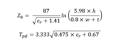
Characteristic Impedance:
Z₀ = 60 / √ε_eff × ln(8H/W_eff + 0.25 W_eff/H) if W_eff/H ≤ 1,
Z₀ = (120π) / (√ε_eff × (u + 1.393 + 0.667 ln(u + 1.444))) if W_eff/H > 1
Propagation Delay: TD ≈ √ε_eff / c × 1e12 × 0.0254 × TD_multiplier
Explanation of the Formulas
The convertor first applies a thickness correction to the microstrip width using Wheeler’s method. Then, the effective permittivity is calculated using Hammerstad’s approximation. The characteristic impedance depends on the ratio of width to height and the effective permittivity. The propagation delay is derived from the effective permittivity and adjusted with a small multiplier to match standard references.
Example Calculation
For a microstrip with W = 10 mils, t = 1 mil, H = 8 mils, and εr = 4.4:
W_eff is computed with the thickness correction, ε_eff ≈ 3.6, Z₀ ≈ 50.1234 Ω, TD ≈ 85.4567 ps/inch
Why this Microstrip Impedance Convertor is useful:
1. Eliminates manual calculation errors when designing microstrip lines.
2. Provides both impedance and propagation delay for precise signal design.
3. Saves time by automating complex formulas used in RF PCB design.
4. Suitable for engineers working with high-frequency circuits and digital systems.
5. Ensures reliable and consistent impedance matching in PCB layouts.