DEMOSFET.
Demosfet: depletion enhancement metal oxide semiconductor field effect transistor
Field-effect transistors (fet) is a type of transistor commonly used for weak signal amplification (for example, to amplify wireless signals).
The device can amplify analog or digital signals.
It can also switch dc or function as an oscillator.
In the fet, current flows along a semiconductor path called a channel.
At one end of the channel, there is an electrode called the source.
At the other end of the channel, there is an electrode called a sewer.
The physical diameter of the fixed line, but the effective electric diameter can be varied by applying voltage to a control electrode called a gate.
The conductivity of the fetus depends, at a particular time, on the diameter of the power line.Small changes in the gate voltage can cause large variations in the current from the source to the drain.This is how the fet amplifies signals.The fetus has several advantages and some disadvantages relative to bipolar transistors.Field effect transistors are preferred for weak signal work, for example in wireless communications and broadcast receivers.
They are also preferred in circuits and systems requiring high impedance.
The fetus is not, in general, used for high power amplification, as required in large wireless communications and broadcast transmitters.Field-effect transistors are fabricated onto silicon integrated circuit (ic) chips.One ic can contain thousands of fets, along with other components like resistors, capacitors, and diodes.Field-effect transistors exist in two major classifications.
The gate field effect transistors are the simplest types of transistor-effect fields. they are a three-terminal semiconductor device that can be used as an electronically controlled switch, amplifier, or voltage-controlled resistor.
Junction junction has a channel of n-type semiconductor (n-channel) or p-type semiconductor (p-channel) materials; gates are made of opposite semiconductor types.
In p-type materials, the electrical charge is carried out primarily in the form of electron defects called holes.
In n-type material, the charge carriers are primarily electrons.
In a jfet, the intersection is the boundary between the channel and the gate.
Usually, the p-n connection is bias-back (dc voltage applied) so that no current flows between the channel and gate.
However, under some conditions there is a small current through the junction during part of the input signal cycle.
We know that when the gate is biased negatively with respect to the source in the n-channel jfet, the width of the depletion region increases. increased depletion area reduces channel thickness, which increases its durability. the net result is that the current drain ID is reduced.
If the polarity vgg is reversed so as to apply a positive bias to the gate with respect to the source, the p -n connection between the gate and the channel will advance forward. because the forward bias reduces the width of the depletion region, the channel thickness will increase with the corresponding channel resistance decrease. as a result, the current drain id will increase beyond the value of idss jfet.
The normal operation of a jfet is in operating mode of depreciation. However, as discussed above, it is also possible to improve the conductivity of the jfet channels. however, the forward bias of the silicon p-n connection is usually limited to a maximum of 0.5 v (more conservative limits are 0.2 v) thus limiting the gate current.
As we have seen, the bigger the id compared to the id, the larger the gm trans conductance. we have seen before that the voltage gain is directly proportional to gm. so, in general, the higher the gm, the better. this is one of the advantages of being able to improve the channel.
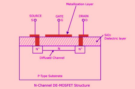
O in mosfet, channel can be either n-type or p-type semiconductor.The gate electrode is a piece of metal whose surface is oxidized.The oxide layer electrically insulates the gate from the channel.For this reason, the mosfet was originally called an isolated gate-fet (igfet), but the term is now rarely used.
Because the oxide layer acts as a dielectric, there is basically no current between the gate and the channel during each part of the signal cycle.This gives the mosfet an extremely large input impedance.Because the oxide layer is very thin, the MOSFET is susceptible to damage by electrostatic charge.Special precautions are necessary when handling or transporting mos devices.

